ASU will be home to semiconductor research and development facility

Add Axios as your preferred source to
see more of our stories on Google.
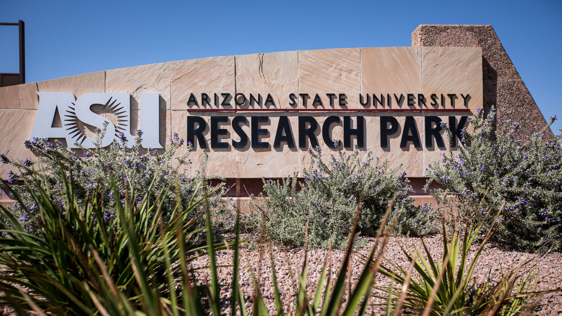
ASU's Research Park in Tempe will be home to a new research and development facility for semiconductor manufacturing and advanced packaging. Photo courtesy of Arizona State University
The Valley's booming semiconductor industry is growing again, with the federal government choosing ASU as one of three manufacturing and advanced packaging research and development facilities.
Why it matters: Arizona is making a name for itself as a semiconductor hot spot, and the addition of a national research facility will contribute to the industry's local growth.
- The National Institute of Standards and Technology (NIST) touted it as the world's first such facility.
- Arizona Commerce Authority spokesperson Patrick Ptak told Axios the facility will attract companies from around the world that want to use it to test new innovations.
State of play: The U.S. Department of Commerce and Natcast, which operates the National Semiconductor Technology Center (NSTC), announced Monday that their third flagship CHIPS for America R&D facility will be located at ASU Research Park.
- The facility will be used to develop and test new materials, devices and advanced packaging solutions, according to the NIST.
- The project will be funded by the CHIPS and Science Act, which has been a boon to Arizona's semiconductor industry.
- Albany, New York, and Sunnyvale, California, will host the other two CHIPS R&D flagship facilities.
Zoom in: ASU's site will conduct research on manufacturing and advanced packaging for 300mm front-end semiconductors. "Front-end" refers to the process to convert a blank semiconductor wafer to a completed wafer.
- Advanced packaging allows multiple semiconductor chips to be combined in a way that mitigates heat and improves performance.
- The facility will provide research and development opportunities "that would not be feasible at a manufacturing site, including novel materials and device architectures," per NIST.
What's next: The facility is expected to become operational in 2028.
What they're saying: "The most advanced microchips in the world that power everything from AI to quantum computing will now be able to be developed, tested, manufactured and packaged in our state," said Democratic U.S. Sen. Mark Kelly, a sponsor of the CHIPS Act.
- "This state-of-the-art research facility will be a beacon of semiconductor innovation, attracting companies from around the world to Arizona to test and prototype leading-edge technologies," said Republican U.S. Rep. Abraham Hamadeh.
The big picture: Taiwan Semiconductor Manufacturing Co. (TSMC) is building a massive facility in north Phoenix that's expected to be home to three plants by decade's end.
- TSMC's facility has attracted various semiconductor-related companies to the Valley and fueled other projects, including a $2 billion advanced packaging facility that Tempe-based Amkor Technology Inc. is building in Peoria.
- Ptak said the facility "amplifies Arizona's national network" and will "attract attention and companies who want to be here to be part of this innovation."